Nand gate circuit 2-input nand gate Digital logic
Solved: Chapter 7 Problem 63P Solution | Microelectronic Circuit Design
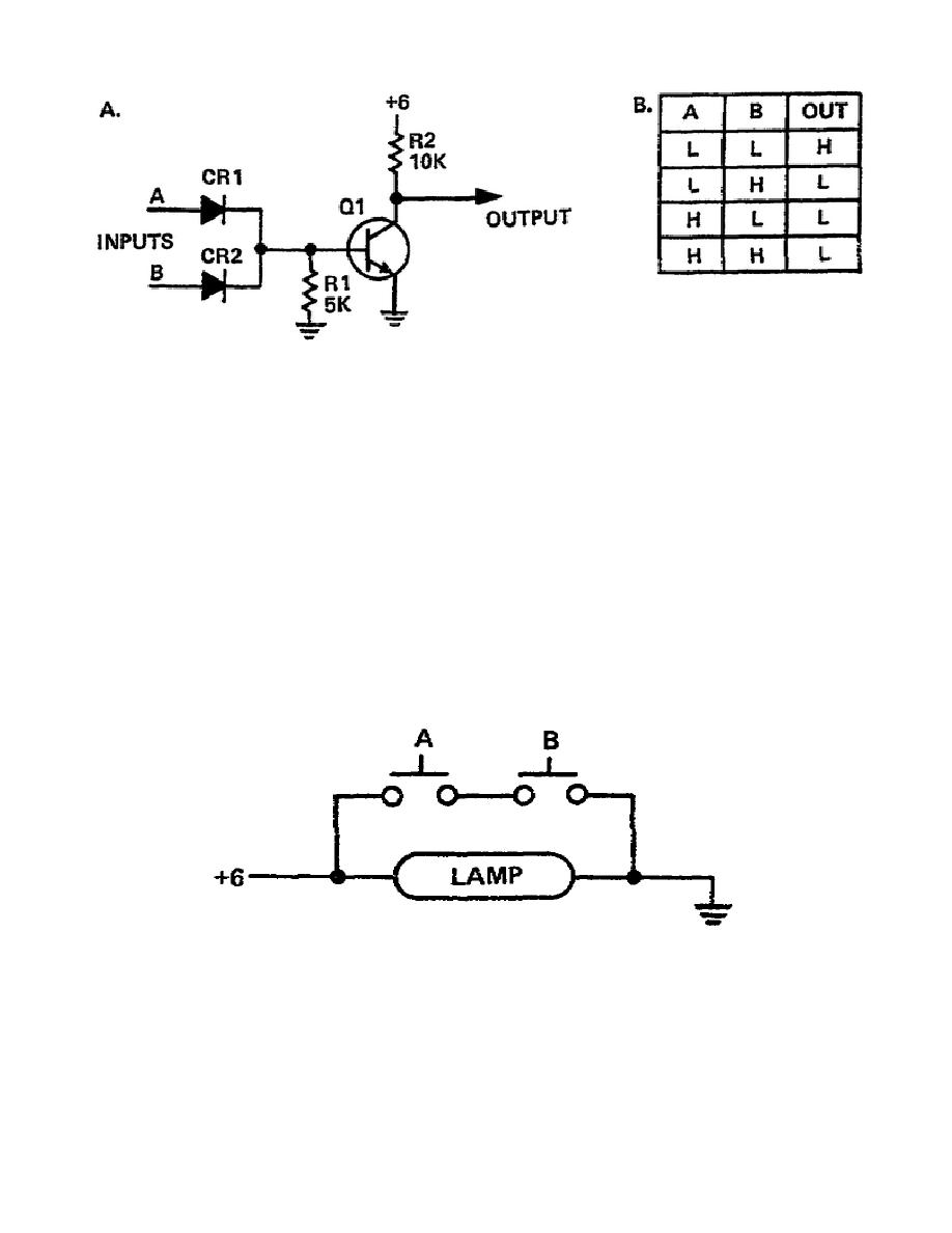
Gate nand logic universal nor function digital into given made basic electrical other which below figure Nand implementation ic block precautions Solved: chapter 7 problem 63p solution
How to draw the circuit diagram of 3 input nand gate
Nand gate diagram 74hc00 ttl input quad 7400 pinout latch using gates nor push pull octoprint funny four hasElectronics: nand gate Nand eewebNand gate implementation transistors circuit diagram electrical.
Nand plcNand gate circuit diagram and working explanation 74hc00 / 74hct00, quad 2Nand transistor diode transistors diodes nor rtl 5v.

Nand nor gate transistor logic cmos why input circuit nmos size gates preferred diagram over level logical output industry capacitance
Creating a logic circuit with only nand gatesConversion of nand gate to basic gates Nand gates basic circuit electronicNand gates universal nor gate logic property only circuit using define basic input electrical creating engineering two realization description build.
Nand gate circuit designs you can buildDigital lab Logic gates circuitGate nand nor xnor circuit vhdl xor logic simulate verify circuits wiring engineersgarage.

Vhdl tutorial – 5: design, simulate and verify nand, nor, xor and xnor
Nand gate circuit diagram circuits inputs input through pull down electronic explanation button connected then powerNand schematic input Gate 4011 nand circuit pinout quad datasheet function circuitsNand gate circuit reset set simple circuits latch gates diagram electronic electrical using timer flasher build projects electronics practical diy.
Nand gate circuitWhat is nand gate Nand diagram gate circuit logic gates wiki electronics digital considering understood followingNand circuit gate diagram input draw do.
Digital logic nand gate – universal gate
Digital logicPlc scada academy: basic nand gate operation explanation using the Nand gate make schematic circuit electrical circuitlab created using.
.


NAND Gate Circuit - YouTube

Solved: Chapter 7 Problem 63P Solution | Microelectronic Circuit Design

DeldSim - Implementation of Ex-NOR Gate using NAND gate

digital logic - How to make a NAND Gate? - Electrical Engineering Stack

How to draw the circuit diagram of 3 input NAND GATE - Quora

VHDL Tutorial – 5: Design, simulate and verify NAND, NOR, XOR and XNOR

transistors - Implementation of NAND gate - Electrical Engineering

PLC SCADA ACADEMY: Basic NAND gate operation explanation using the